Printed Circuit Boards - Construction Materials
There is a lot of confusion amongst students and fresh graduates with regards to the PCB fabrication process. I have accumulated some knowledge from around the web (References: Link1 | Link2) and added some of my own here to serve as a ready reckoner of a few important notes regarding PCBs.
PCB Process in Brief:
Copper laminate -> Drill board -> Deposit Copper -> Photolithography -> Tin lead plate or finishing -> Etching -> Hot air level -> Solder mask -> Electrical Testing -> Routing and V-scoring -> Product inspection -> Final cleanning -> Packaging.
PCB Terminology
- Base Laminate - That sheet of insulating material (a.k.a. dielectric) to which a thin copper foil is affixed on either or both sides. This material is constructed by repeatedly uniting two or more layers of material together. The process of creating a laminate is lamination, which in common parlance refers to the placing of something between layers of plastic and glueing them with heat and/or pressure, usually with an adhesive. Refer wikipedia entry for Laminates. Base Laminates are of many types (depending on the materials used to make them) - FR2, FR4, CEM1 etc.
- Pre-preg - stands for "pre-impregnated". The Base Laminate is made of insulating layers of a particular dielectric typically laminated together with epoxy resin prepreg. A pre-preg is a sheet of material that has been impregnated with a resin cured to an intermediate stage. Read "How's FR4 Made" for a clearer explanation.
- Epoxy - Used to bind the various dielectric plies together during the process of lamination. Eead the Wikipedia article for a clearer picture.
- PTH or Plated Through Hole - A hole with the plated copper on its sides to provide electrical connections between conductive patterns present on two or more conducting layers of a PCB. There are two types of PTH - one is for mounting leaded components and may or may not create electrical connections between patterns of the two or more conducting layers through which it passes. The other one (called a via) is not used for mounting components and is used only for the purpose of creating electrical connections between patterns (i.e., traces) on two or more conducting copper layers.
- Blind via - A via hole that does not pass completely through the printed circuit board. A blind via starts from one side or another.
- Buried via - A via connects two or more inner layers but no outer layer, and cannot be seen from either side of the board.
- Pad - The portion of the conductive pattern on printed circuits designated for the mounting or attachment of components.
- Bare Board - A finished printed circuit board (PCB) that has no components mounted yet.
- FR2 (a.k.a. Paper Phenolic)The base is composed of multiple plies of paper impregnated with flame retarding phenolic resin. The major advantage of the material is the low cost, good electrical and punching performance. In India, you will find most cheap single sided PCBs made of this material. It is brown in colour. Wikipedia article on FR-2
- FR3 (a.k.a. Paper Epoxy)The same as FR2 but the paper is impregnated with an epoxy resin providing better electrical and mechanical properties. The material is used in TV, computer and telecommunication applications.
- CEM1The material is a composite with paper as the core and woven glass cloth on the outer surfaces - each impregnated with epoxy resin. The material can provide the punching characteristics of the previous materials and many of the electrical and mechanical advantages of FR4 laminate. The surface of this material is white in colour because of the woven glass but brown on the sides because the core is made of paper.
- CEM3This material again has woven glass cloth on both outer surfaces but with non-woven glass in the core. It has epoxy resin and is more suitable for through plated holes than CM1.
- FR4 (a.k.a. Glass Epoxy)By far the most often specified product produced from multiple layers of woven glass cloth impregnated with epoxy resin. It has superior properties to the other laminate sheets with a higher price tag. The glass transition (Tg) temperature of the material is between 125-140°C. This laminate is mainly used for plated through and multilayer functions. It is used in all types of electronic products including military space and advanced computer systems. Wikipedia rticle on FR-4
- FR5Basically the material is the same as FR4 but with a modified epoxy filling which improves the Tg to between 150-165°C. This improves the thermal stability of the product. Generally used where a product is required to work at higher temperature.
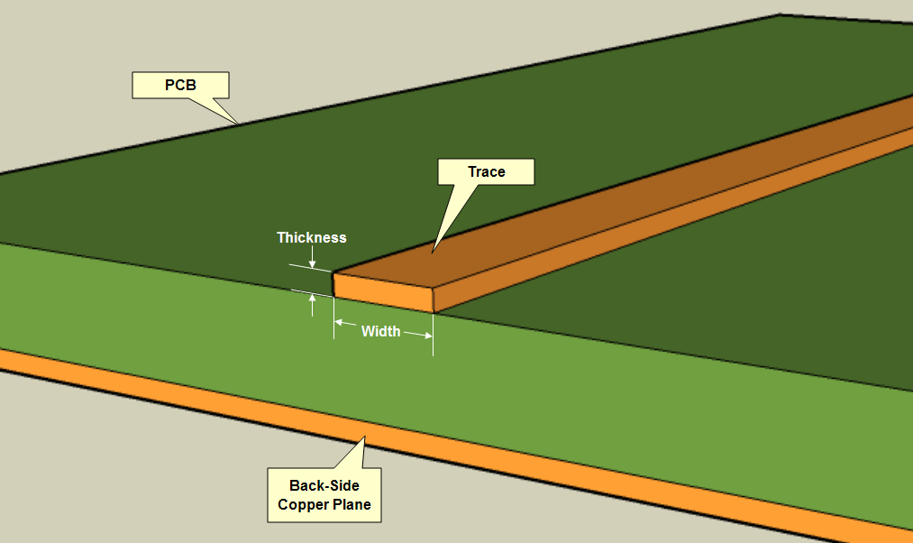
Copper Thickness
The copper in a PCB is rated in ounces, and represents the thickness of 1 ounce of copper rolled out to an area of 1 square foot. For example a PCB that uses 1 ounce copper has a thickness of 1.4 mils. mil is a unit of measurement of length. 1 mil = 1/1000th of an inch. 1 inch is 2.54 cm. PCBs are available with varying copper thicknesses:
1/2 ounce per square feet > 0.7 mils or 18 microns thick1 ounce per square feet > 1.4 mils or 36 microns thick2 ounce per square feet > 2.8 mils or 72 microns thick
Photos
Here is a photo of 3 PCBs of the same design fabricated using three different base laminates. All PCBs are 1.6mm thick and have tracks etched only on a single side. A green colour solder maske is applied to the side on which tracks are etched. The copper thickness is 36 microns but after tinning, the thickness rises to about 70 microns. Tinning is the process of applying a thin layer of Tin to the copper pads whhich stay exposed even after the solder mask is applied. Tinning protects the pads which would have been otherwise oxidised and would prevent solder from sticking to the copper. (Copper gets oxidized when it comes in contact with air, Tin doesn't get oxidised) The dimensions of the PCBs are 160 mm by 103 mm

Top Side (Component Side)

Bottom Side (Solder Side)

Side View
The PCBs featured in the photos are of the same design : "89C51/89C2051 General Purpose PCB" The PCBs and the components in a kit form are available from:
Visha Electronics Corporation
| Address: | 1st Floor, Kalpana Building, 349 Lamington Road, Opp. Police Station, Mumbai 400 007, INDIA |
| Phone: | +91 22 23862650 +91 22 23862622 |
| Fax: | +91 22 23884401 |
| Email: | info@vishaworld.com |
Prices of the Bare PCB as of August 2010:
FR2 Version - 50 Indian Rupees
CEM1 Version - 70 Indian Rupees
FR4 Version - 90 Indian Rupees
A page describing the assembly and use of this PCB for developing the projects around the 8051 microcontroller is located here.
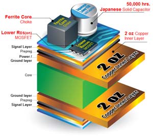
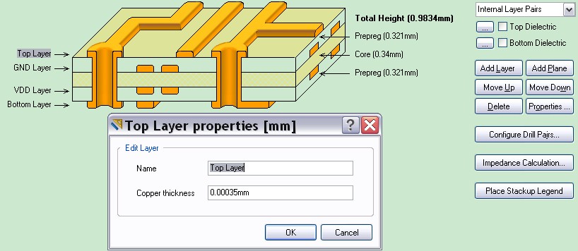
Links to 3D images of PCB cross-sections found on the web:
Image1 | Image2 | Image3 | Image4 | Image5 | Image6
Also checkout the course website for "Concepts of PCB Design" @ University of Bolton


Comments
Post a Comment